2021-01-06 ProPowertek
With the booming development of 5G, IoT and electric vehicles, the requirements for low power consumption are getting more and more demanding, which makes power semiconductors become an irresistible and essential component for these industries. To meet the requirements of customers, Prosperity Power Technology Inc. (abbreviated as ProPowertek) announces today (January 6, 2021) that it has made a breakthrough in 1.5 mil (38um) taiko wafer with high wafer strength, which has been recognized by customers.
ProPowertek pointed, wafer thinning has been the most direct and effective process improvement in cutting power consumption and input impedance of power semiconductors which not only reduce packaging dimension but also extends the operating life of wafers by lowering RDS (on) and heat accumulation.
However, the MOSFET foundries are facing a challenge of balancing thinness and strength of wafers to minimize the risks of soaring rate of broken
wafers.ProPowertek is not only to exclusively develop the thinning technology for wafers 2mil(50um), 1.5mil(38um), and even 0.4mil(10um) thick, but also strengthen wafers by reducing stress accumulation at the damage layer with its optimized process.
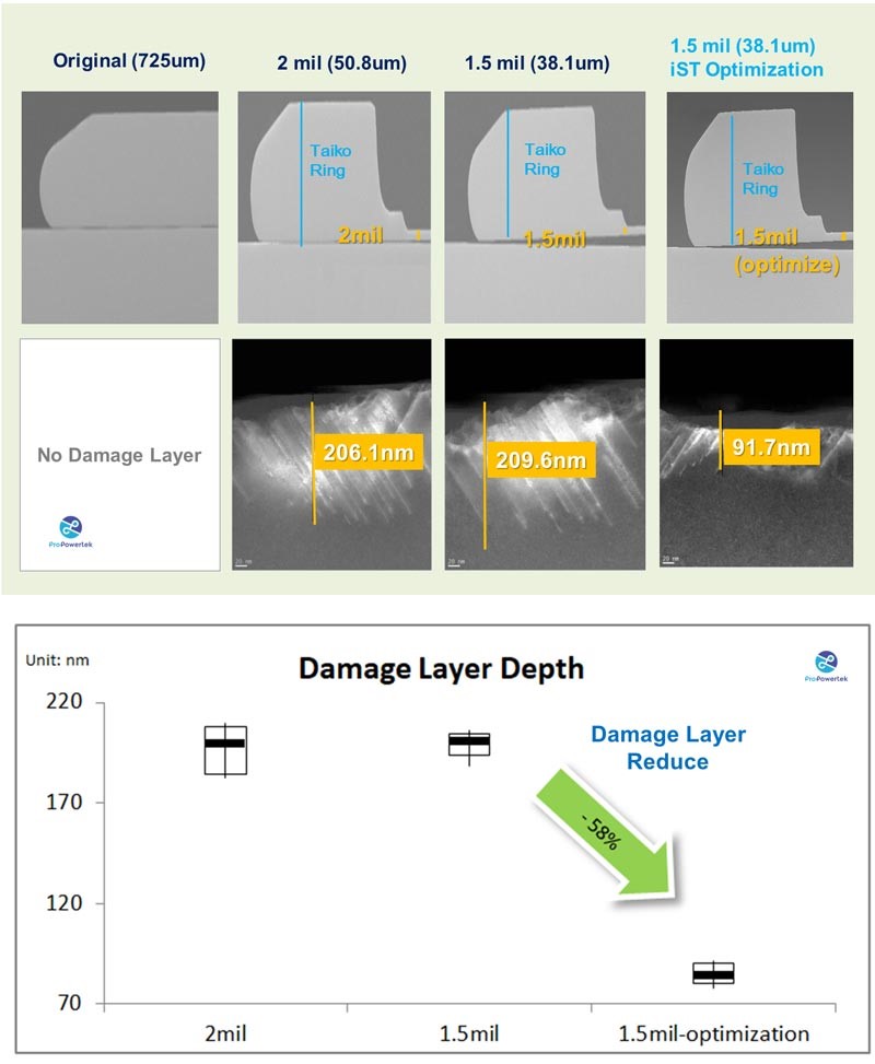
Figure: TEM maps of damage layers in thickness of 2mil, 1.5mil and 1.5mil after optimization by using control wafers
ProPowertek can provide you with customized solutions to enhance your wafer for Power MOSFET/IGBT and other components. Should you have any inquiries, just ring Mr. Liu at +886-3-579-9209 EXT 5001 or email us at contact@propowertek.com