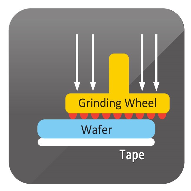
During the back grinding (BG) of the wafer thinning process, the wafer is quickly and accurately ground with a grinding wheel to remove the damage caused by grinding and stress release.
What ProPowertek can do for you?
In the complete BGBM process, the first step is wafer thinning. After Grinding and etching, it can provide customers with a thickness to 100um, remove the damaged layer and reduce stress.
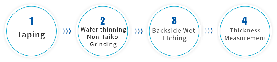
Wafer thining/Non-Taiko Grinding Process
Taping wafers with tapes determined by wafer features and passivation layers by front end foundries; then, perform Non-Taiko Grinding / Conventional Grinding and Backside Wet Etching in sequence before thickness measurement.
The Superiority of ProPowertek
▶ Employ fully automatic DISCO equipment for precisely controlled grinding ▶ Provide spin etching tools to perform surface processes for N- or P-type wafers as required by customers ▶ Far outperforms the dial gauge widely adopted by the industry with non-contact optical and high-precision measurement ▶ A team of engineers with diversified experts including front end wafer foundry, wafer thinning and backend packaging house, knowledgeable and experienced in process integration and analysis in phases from front through middle to back and well-prepared to assist customers in accelerated development, troubleshooting, and mass production stabilization.
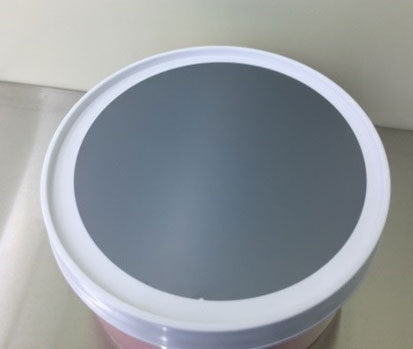
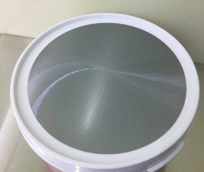
Case Sharing
Wafers After Grinding and Etching
Post-grinding wafers
Post-etching wafers
Application
⏺︎ Existing thickness options: ≧100um with thickness subject to customer requirements
⏺︎ Applicable to 8″/6″ P- or N-type wafers