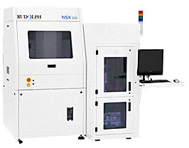
ProPowertek is equipped with high-resolution Automatic Optical Inspection (AOI) systems, offering customers inspection services for both thick and thin wafers during incoming and outgoing quality control, as well as inspection after wafer frame mounting.
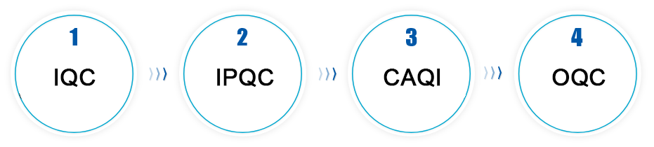
▶ ProPowertek is equipped with AOI (Automatic Optical Inspection) systems that support optical inspection at various stages. IQC (Incoming Quality Control) ensures upstream wafer quality, while in-process and outgoing inspections guarantee process reliability. ▶AOI inspection enables better yield control by integrating upstream or CP (Chip Probing) wafer test maps. This supports downstream packaging by enabling good die selection, helping to reduce packaging costs. ▶ Fully automated AOI reduces human contact, improving reliability and efficiency. It also enhances defect analysis by collecting precise abnormality locations, significantly shortening root cause analysis time. ▶ Our engineering team has diverse backgrounds, including experience in front-end wafer foundries, wafer thinning processes, and back-end packaging houses. This cross-domain expertise enables rapid development, effective problem-solving, and stable mass production support for our customers
Case Sharing
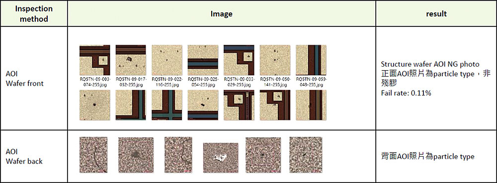
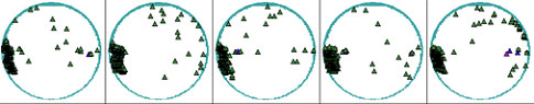
Using AOI to Identify Die Defects and Control Yield
AOI enables detection of common defect distribution patterns, accelerating failure analysis and process convergence.
Application
⏺︎ Standard 8″ Wafers, Thick/Thin Wafers, Frame-Mounted Wafers, Post-Dicing Wafers, and Post-CP (Chip Probing) Wafer Inspection